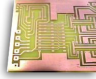
Printed Circuit Board (PCB) is a mechanical assembly
consisting of layers of fiberglass sheet laminated with etched
copper patterns. It is used to mount electronic parts in a rigid
manner suitable for packaging. Also known as a Printed Wiring Board
(PWB).
<!– ——————————————————– –>Project
A schematic diagram must be made available that shows the
connection of the parts on the board. Each part on the schematic
should have a reference designator that matches the one shown on
the Bill of Materials (BOM). Many schematic layout programs will
allow automatic generation of the BOM.
Part List - Bill
of Materials (BOM)
The parts to be mounted on the PCB should be detailed on the parts
list. Each part should be identified by a unique reference
designator and a part description (i.e. a resistor might be shown
as reference designator “R1” with a description of “1/2 Watt Carbon
Film resistor”). Any additional information useful to the assembly
process can be included on this list, such as mounting hardware,
part spacers, connector shrouds, or any other material not shown in
the schematic diagram.
Choose components
from Data Sheets
Part manufacturers provide data sheets to be used by the circuit
designer to select parts for the circuit. If we are to be able to
design the PCB, these sheets should also have the physical
dimensions of the part included. Normally you could find datasheets
from manufacturers web sites. If each part type to be used on the
board does not have a data sheet, you should procure a sample part
you can measure to define this data yourself. This measurment
method is far less accurate than using the part manufacturer’s
information, especially if there is a large tolerance on the part,
but it is better than just guessing.
Choose Board type
and dimension
A functional PCB is not a finished product. It will always require
connections to the outside world to get power, exchange
information, or display results. It will need to fit into a case or
slide into a rack to perform it’s function. There may be areas that
will require height restrictions on the board (such as a battery
holder molded into the case or rails in a rack the board is
supposed to slide into). Tooling holes and keep-out areas may be
required in the board for assembly or manufacturing processes. All
these outside factors need to be defined before the board can be
designed, including the maximum dimensions of the board and the
locations of connectors, displays, mounting brackets, or any other
external features.
The function of a PCB includes the thickness of the copper
laminated to the surfaces. The amount of current carried by the
board dictates the thickness of this copper foil. Normally the
thickness of the copper foil is standard.
Also you can choose between different board types for material and
number of layers:
- Material
- Fibreglass

Fibreglass-resin laminate (FR4). A rigid PCB of thickness 1.6mm (conventional) or 0.8mm. - Phenolic
As distinct from Fibreglass, Phenolic is a cheaper PCB laminate material. A rigid PCB of thickness 1.6mm (conventional) or 0.8mm. - Single side Laminate

One layer of copper. Normally the wire-leaded components must be mounted on only one side of the PCB, with all the leads through holes, soldered and clipped.
You can also mount the components on the track surface using Surface Mount Technology (SMT) or Surface Mount devices (SMD). Surface mount circuitry is generally smaller than conventional. Surface mount is generally more suited to automated assembly than conventional. In practice, most boards are a mix of surface mount and conventional components. This can have its disadvantages as the two technologies require different methods of insertion and soldering. Conventional circuitry is generally easier to debug and repair. - Double sided Laminate

Two layers of copper, one each side of the board. The components must be mounted on only one side of the PCB but you can also mount components on both sides of the PCB. Normally only surface mount circuitry would be mounted on both sides of a PCB. The components must be mounted using both through-holes tecnology or Surface Mount Technology (SMT) or Surface Mount devices (SMD). Conventional circuitry is generally easier to debug and repair. - Multi-Layer

A PCB Laminate may be manufactured with more than two layers of copper tracks by using a sandwich construction. The cost of the laminate reflects the number of layers. The extra layers may be used to route more complicated circuitry, and/or distribute the power supply more effectively.
Draw the PCB
layout
The PCB layout can be draw either manually or by ECAD (Electronic -
Computer Aid Design) software. The manual process is useful and
quick only for very easy PCBs, for more complex PCBs I suggest the
second way. Nowadays inexpensive computer software can handle all
aspect of PCBs pre-processing. Also is available expensive
professional computer software that can direct control the
fabrication processing tools (e.g.: drilling machine).
A few general rules of thumb that can be used when laying out PC
boards are:
Placing Components
Generally, it is best to place parts only on the top side of the
board.
First place all the components that need to be in specific
locations. This includes connectors, switches, LEDs, mounting
holes, heat sinks or any other item that mounts to an external
location.
Give careful of thought when placing component to minimize trace
lengths. Put parts next to each other that connect to each other.
Doing a good job here will make laying the traces much easier.
Arrange ICs in only one or two orientations: up and down, or, right
and left. Align each IC so that pin one is in the same place for
each orientation, usually on the top or left sides.
Position polarized parts (i.e. diodes, and electrolytic caps) with
the positive leads all having the same orientation. Also use a
square pad to mark the positive leads of these components.
You will save a lot of time by leaving generous space between ICs
for traces. Frequently the beginner runs out of room when routing
traces. Leave 0.350" - 0.500" between ICs, for large ICs allow even
more.
Parts not found in the component library can be made by placing a
series of individual pads and then grouping them together. Place
one pad for each lead of the component. It is very important to
measure the pin spacing and pin diameters as accurately as
possible. Typically, dial or digital calipers are used for this
job.
When choosing a pad and hole size for the pin of component, keep in
mind that the hole size refers to the drill size used when the
board is made. After the hole is plated, the diameter will shrink
by 0.005" - 0.007". To the pin diameter, add 0.008" or more when
selecting a hole size.
After placing all the components, print out a copy of the layout.
Place each component on top of the layout. Check to insure that you
have allowed enough space for every part to rest without touching
each other.
Placing Power and Ground
Traces
After the components are placed, the next step is to lay the power
and ground traces. It is essential when working with ICs to have
solid power and ground lines, using wide traces that connect to
common rails for each supply. It is very important to avoid snaking
or daisy chaining the power lines from part-to-part.
One common configuration is to use the bottom layer of the PC board
for both the power and ground traces. A power rail can be run along
the front edge of the board and a ground rail along the rear edge.
From these rails attach traces that run in between the ICs. The
ground rail should be very wide, perhaps 0.100", and all the other
supply lines must be 0.050". When using this configuration, the
remainder of the bottom layer is then reserved for the vertical
signal traces.
Placing Signal Traces
The process to connect the parts together is known as routing and
can be done manually or automatically.
If you use authorouter software it’s a good idea to route critical
signals by hand. This allows the signal to be routed with less
bends and vias than if the authorouter does it. Some signals may
require special treatment such as grounding or specific lengths
that may be easier to do before authorouting than after. These
traces should be flagged as fixed so the authorouter doesn’t move
them.
When placing traces, it is always a good practice to make them as
short and direct as possible.
Use vias (also called feed-through holes) to move signals from one
layer to the other. A via is a pad with a plated-through hole.
Generally, the best strategy is to layout a board with vertical
traces on one side and horizontal traces on the other. Add via
where needed to connect a horizontal trace to a vertical trace on
the opposite side.
A good trace width for low current digital and analog signals is
0.012".
Traces that carry significant current should be wider than signal
traces.
The table below gives rough guidelines of how wide to make a trace
for a given amount of current.
| Trace Width [inches] | Current [A] |
|---|---|
| 0.010 | 0.3 |
| 0.015 | 0.4 |
| 0.020 | 0.7 |
| 0.025 | 1.0 |
| 0.050 | 2.0 |
| 0.100 | 4.0 |
| 0.150 | 6.0 |
When placing a trace, it is very important to think about the space
between the trace and any adjacent traces or pads. You want to make
sure that there is a minimum gap of 0.007" between items, 0.010" is
better. Leaving less blank space runs the risk of a short
developing in the board manufacturing process. It is also necessary
to leave larger gaps when working with high voltage.
It is a common practice to restrict the direction that traces run
to horizontal, vertical, or at 45 degree angles.
When placing narrow traces, 0.025" or less, avoid sharp right angle
turns. The problem here is that in the board manufacturing process,
the outside corner is often etched too narrow. The solution is to
use two 45 degree bends with a short leg in between.
It is good idea to place text on the top layer of your board, such
as a product or company name. Text on the top layer can be helpful
to insure that there is no confusion as to which layer is which
when the board is manufactured.
Checking Your Work
After all the traces are placed, it is best to double check the
routing of every signal to verify that nothing is missing or
incorrectly wired. Do this by running through your schematic, one
wire at a time. Carefully follow the path of each trace on your PC
layout to verify that it is the same as on your schematic. After
each trace is confirmed, mark that signal on the schematic with a
yellow highlighter.
Inspect your layout, both top and bottom, to insure that the gap
between every item (pad to pad, pad to trace, trace to trace) is
0.007" or greater.
Check for missing vias. An easy way to check for missing via is to
first print the top layer, then print the bottom. Visually inspect
each side for traces that don’t connect to anything. When a missing
via is found, insert one.
Check for traces that cross each other. This is easily done by
inspecting a printout of each layer.
Metal components such as heat sinks, crystals, switches, batteries
and connectors can cause shorts if they are place over traces on
the top layer. Inspect for these shorts by placing all the metal
components on a printout of the top layer. Then look for traces
that run below the metal components.
Draw Fabrication
scheme
The fabrication drawing should show the dimensions of the board in
reference to the datum tool hole. It should also show a graphic
representation for each hole on the board, using a different symbol
for each hole size and including a table showing the quantity of
each hole size. This drawing will be used by the board manufacturer
in addition to the data files generated in the post-processing
phase.
Draw Assembly
scheme
You may also need to create an assembly drawing to aid in building
and repairing the board. This should show the outlines of the parts
on the board, including their reference designators. It also should
contain any special assembly instructions, such as mounting
hardware and connector shells. Many companies require these
drawings, others just use copies of the silkscreen legend.
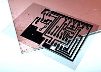
Different methods to make PCBs
[Etching]
Etching is probably the easiest and most cost effective.
Etching is the process of chemically removing the unwanted copper
from a plated board. You must put a mask or resist on the portions
of the copper that you want to remain after the etch. These
portions that remain on the board are the traces that carry
electrical current between devices.
- Ferric
Chloride
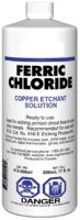
It’s messy stuff but easier to get and cheaper than most alternatives. It attacks ANY metal including stainless steel, so when setting up a PCB etching area, use a plastic or ceramic sink, with plastic fittings & screws wherever possible, and seal any metal screws etc. with silicone. If copper water pipes may get splashed or dripped, sleeve or cover them in plastic. Fume extraction is not normally required, although a cover over the tank or tray when not in use is a good idea.
You should always use the hexahydrate type of ferric chloride, which is light yellow, and comes as powder or granules, which should be dissolved in warm water until no more will dissolve. Adding a teaspoon of table salt helps to make the etchant clearer for easier inspection.
Anhydrous ferric chloride is sometimes encountered, which is a green-brown powder. Avoid this stuff if at all possible use extreme caution, as it creates a lot of heat when dissolved - always add the powder very slowly to water, do not add water to the powder, and use gloves and safety glasses You may find that solution made from anhydrous FeCl doesn’t etch at all, if so, you need to add a small amount of hydrochloric acid and leave it for a day or two.
Always take extreme care to avoid splashing when dissolving either type of FeCl - it tends to clump together and you often get big chunks coming out of the container & splashing into the solution. It will damage eyes and permanently stain clothing and pretty much anything else - use gloves and safety glasses and wash off any skin splashes immediately
If you’re making PCBs in a professional environment, where time is money, you really should get a heated bubble-etch tank. With fresh hot ferric chloride, a PCB will etch in well under 5 minutes, compared to up to an hour without heat or agitation. Fast etching also produces better edge quality and consistent line widths.
If you aren’t using a bubble tank, you need to agitate frequently to ensure even etching. Warm the etchant by putting the etching tray inside a larger tray filled with boiling water - you want the etchant to be at least 30-60°C for sensible etch times.
For more information on Ferric Chloride click here. - Ammonium
Persulphate.

Sodium Persulphate Etchant is supplied as a dry, easily mixed etchant for copper clad printed circuit boards and other copper bearing materials. When used in conjunction with the catalyst, a very constant etch rate can be maintained throughout the life of the bath. After mixing, the bath has a practical life of about three (3) weeks and a copper capacity of approximately four to five (4-5) ounces of copper per gallon (29.96 - 37.45 grams / liter) of etchant.
Sodium Persulphate Etchant, when compared to Ferric Chloride and other copper etchants, has several distinct advantages.
Cleanliness: Sodium Persulphate will not stain clothes, skin or tanks.
Rinsing: Sodium Persulphate rinses easily and leaves no residue in plain water.
Etching speed: Sodium Persulphate attains a fast etching speed and with regular additions of the catalyst, maintains a relatively even etching rate throughout its entire mix life.
However, as with all etchants, Sodium Persulphate has several disadvantages:
Short active life: once Sodium Persulphate is mixed, it has a tank life of three (3) weeks, maximum, whether or not it is used.
Aggressiveness: Sodium Persulphate will attack natural fibers such as cotton, wool and linen.
For more information on Ammonium Persulphate click here.
Etching
Possible etching solutions include the following:
There are different methods to prepare the board before the etching process:
<!– ——————————————————– –>- Spray photo sensitive resist
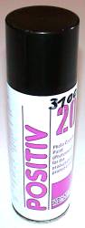
It’s very hard to use, as you always get dust settling on the wet resist. I wouldn’t recommend it unless you have access to a very clean and ventilated area or drying oven, or only want to make low-resolution PCBs. In any case, to use the positive photoresist spray you must:
0) Make a lot of practice.
1) Cleaning: Degrease the surface before application of product.
2) Application of the coating: Spray briefly the PC board in a subdued light from a distance of aprox. 20 cm until the coating will be visible. This work must be carried out in absolutely dust-free conditions. Then the coating must be dried (20°C = 24 h, better 70°C = 15 min).
Note that the photoresist spray are normally EXTREMELY FLAMMABLE. - Pre-coated photoresist fibreglass (FR4) board
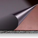
Always use good quality pre-coated photoresist fibreglass (FR4) board. Check carefully for scratches in the protective covering, and on the surface after peeling off the covering. You don’t need darkroom or subdued lighting when handling boards, as long as you avoid direct sunlight, minimize unnecessary exposure, and develop immediately after UV exposure. - Clear acetate OHP transparencies
These may seem like the most obvious candidate, but are expensive, tend to crinkle or distort from laser printer heating, and toner/ink can crack off or get scratched very easily. - Polyester drafting film
It's good but expensive, the rough surface holds ink or toner well, and it has good dimensional stability. If used in a laser printer, use the thickest stuff you can get, as the thinner film tends to crinkle too much due to the fusing heat. Even thick film can distort slightly with some laser printers. - Tracing paper
Has good enough UV translucency and is nearly as good as drafting film for toner retention, and stays flatter under laser-printer heat than polyester or acetate film. It's cheap, easily available from office or art suppliers (usually in pads the same size as normal paper sizes). Get the thickest you can find but at least 90gsm (thinner stuff can crinkle), 120gsm is even better but harder to find. - Manual Pen
It’s not a real choice but you can use it to make very low definition PCBs or to retouch a bit your artwork (e.g. closing pinholes). The Pen must be a black permanent marker. - Dry Transfers

It’s slow and expensive method but allows you to draw manually with a good precision or to retouch a bit your artwork. - Pen plotters
Very fiddly and slow, you have to use expensive polyester drafting film (tracing paper is no good as ink flows along the fibres) and you need special inks and expensive ink pens with grooved tips to get acceptable results. Pens need frequent cleaning and clog very easily. - Ink-jet printers
They are so cheap that it’s certainly worth a try, and with as many different media types as you can find, but don’t expect the same quality you can get from lasers. The main problem will be getting an opaque enough black. It may also be worth trying an inkjet print onto paper, which can then be photocopied onto tracing paper with a good quality copier. - Laser printers
Easily the best all-round solution. Very affordable, fast and good quality. The printer used must have at least 600dpi resolution for all but the simplest PCBs, as you will usually be working in multiples of 0.025" (40 tracks per inch). 300DPI does not divide into 40, 600DPI does, so you get consistent spacing and linewidth.
It is very important that the printer produces a good solid black with no toner pinholes. If you’re planning to buy a printer for PCB use, do some test prints on tracing paper to check the quality first. If the printer has a density control, set it to ‘blackest’. Even the best laser printers don’t generally cover large areas (e.g. ground planes) well, but this isn’t usually a problem as long as fine tracks are solid.
When using tracing paper or drafting film, always use manual paper feed, and set the straightest possible paper output path, to keep the artwork as flat as possible and minimise jamming. For small PCBs, remember you can usually save paper by cutting the sheet in half (e.g. cut A4 to A5) you may need to specify a vertical offset in your PCB software to make it print on the right part of the page.
Some laser printers have poor dimensional accuracy, which can cause problems for large PCBs, but as long as any error is linear (e.g. does not vary across the page), it can be compensated by scaling the printout in software. The only time that print accuracy is likely to be a noticeable problem is when it causes misalignment of the sides on double-sided PCBs - this can usually be avoided by careful arrangement of the plots on the page to ensure the error is the same on both layers, for example choosing whether to mirror horizontally or vertically when reversing the top-side artwork. - Typesetters
For the best quality artwork, generate a Postscript file and take it to a DTP or typesetting service, and ask them to do a film of it. This will usually have a resolution of at least 2400DPI, absolutely opaque black and perfect sharpness. Cost is usually 'per page' regardless of area used, so if you can fit multiple copies of the PCB, or both sides onto one sheet, you'll save money. This is also a good way to do the occasional large PCB that won't fit your laser printer, sizes up to A3 are widely available and larger ones can also be done by more specialised services. Typeset artworks are good enough for production PCBs, but many PCB houses nowadays only accept gerber data, as it's easier for them to post-process for step & repeat etc. - Sodium Hydroxide
Sodium Hydroxide is a very bad choice, it’s completely and utterly dreadful stuff for developing PCBs.
Sodium Hydroxide is caustic, very sensitive to both temperature and concentration, and made-up solution doesn’t last long. Too weak and it doesn’t develop at all, too strong and it strips all the resist off. It’s almost impossible to get reliable and consistent results, especially so if making PCBs in an environment with large temperature variations (garage, shed etc), as is often the case for such messy activities as PCB making.
Manually (direct draw)
One way to put a pattern on the board is the direct draw approach.
Using either a resist pen to draw your circuit, or by using
specialty tapes (dry tranfers), donuts and the lot, you layout your
circuit traces directly onto the copper surface of the board. The
pen technique relies on the waterproof nature of the ink and the
tapes as an impervious plastic, both of which prevent the etchant
from getting at the copper beneath, hence, all copper is etched
away except for where the pattern has been drawn. This is the
quickest way to get a circuit pattern on the board, but it is
difficult to position the traces accurately, especially if you are
using any IC packages in your design. Plus, since the ink doesn’t
apply uniformly, there is a risk that the traces will be etched
away since the etchant can get to the copper through an extremely
thin layer of resist. If you make a mistake you have to start all
over again!
For these reason, you can use this method only to make very easy
low-definition PCBs or to retouch a bit your PCB before
etching.
Photographic
I suggest this method to producing consistently high quality
PCBs quickly and efficiently, particularly for professional
prototyping of production boards.
In this method, a board is covered with a resist material that sets
up when exposed to Ultra Violet light. To make a board this way,
you must make a positive UV translucent artwork film of your layout
pattern which is opaque where you want a circuit trace, and clear
where you don’t want a trace. After the photo positive film is made
from your artwork, it is placed onto the photo sensitized board,
and is exposed to the UV. The UV light transmits through the clear
portions of the film and cures the photoresist. After that, the
board is submerged into a developer bath that develops and remove
the sensitized photoresist. The resist that is left is in the shape
of the artwork that represents your circuit. The advantage to this
approach is accurate and neat traces, and once you make the artwork
film, it can be used over and over to make additional boards.
You’ll never get a good board without good artwork, so it is
important to get the best possible quality at this stage. The most
important thing is to get a clear sharp image with a very solid
opaque black.
Nowadays, artwork will almost always be drawn using either a
dedicated PCB CAD program, or a suitable drawing / graphics
package.
The artwork must be printed such that the printed side will be in
contact with the PCB surface when exposing, to avoid blurred edges.
In practice this means that if you design the board as seen from
the component side, the bottom (solder side) layer should be
printed the ‘correct’ way round, and the top side of a double-sided
board must be printed mirrored.
Artwork quality is very dependant on both the output device and the
media used.
- Photoresist PCB
laminates
To transfer the image on the artwork film to the board you must use board treated with a special Photo Copying Paint (Photoresist).
Contrary to what you may think, it is NOT necessary to use a transparent artwork medium, as long as it is reasonably translucent to UV. Less translucent materials may need a slightly longer exposure time. Line definition, black opaqueness and toner/ink retention are much more important. Possible print media include the following:
Print device is fundamental to produce good artwork. Possible print devices include the following:
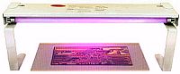
The photoresist board needs to be exposed to ultra-violet light
through the artwork, using a UV exposure box.
UV exposure units can easily be made using standard fluorescent
lamp ballasts and UV tubes. For small PCBs, two or four 8 watt 12"
tubes will be adequate, for larger (A3) units, four 15" 15 watt
tubes are ideal. To determine the tube to glass spacing, place a
sheet of tracing paper on the glass and adjust the distance to get
the most even light level over the surface of the paper. Even
illumination is a lot easier to obtain with 4-tube units. The UV
tubes you need are those sold either as replacements for UV
exposure units, insect killers or ‘black light’ tubes for disco
lighting etc. They look white or occasionally black/blue when off,
and light up with a light purple, which makes flourescent paper
etc. glow brightly. DO NOT use short-wave UV lamps like EPROM
eraser tubes or germicidal lamps, which have clear glass - these
emit short-wave UV which can cause eye and skin damage.
A timer which switches off the UV lamps automatically is essential,
and should allow exposure times from 2 to 10 minutes in 15-30
second increments. It is useful if the timer has an audible
indication when the timing period has completed. A timer from a
scrap microwave oven would be ideal.
Short-term eye exposure to the correct type of UV lamp is not
harmful, but can cause discomfort, especially with bigger units.
Use glass sheet rather than plastic for the top of the UV unit, as
it will flex less and be less prone to scratches.
If you do a lot of double-sided PCBs, it may be worth making a
double-sided exposure unit, where the PCB can be sandwitched
between two light sources to expose both sides simultaneously.
You will need to experiment to find the required exposure time for
a particular UV unit and laminate type, expose a test piece in 30
second increments from 2 to 8 minutes, develop and use the time
which gave the best image. Generally speaking, overexposure is
better than underexposure.
For a single-sided PCB, place the artwork with toner side up on the
UV box glass, peel off the protective film from the laminate and
place it sensitive side down on top of the artwork. The laminate
must be pressed firmly down to ensure good contact all over the
artwork, and this can be done either by placing weights on the back
of the laminate, or by fitting the UV box with a hinged lid lined
with foam rubber, which can be used to clamp the PCB and
artwork.
To expose double-sided PCBs, print the solder side artwork as
normal, and the component side mirrored. Place the two sheets
together with the toner sides facing, and carefully line them up,
checking all over the board area for correct alignment, using the
holes in the pads as a guide. A light box is very handy here, but
it can be done with daylight by holding the sheets on the surface
of a window. If printing errors have caused slight
mis-registration, align the sheets to ‘avarage’ the error across
the whole PCB, to avoid breaking tracks when drilling. When they
are correctly aligned, staple the sheets together on two opposite
sides (3 sides for big PCBs), about 10mm from the edge of the
board, forming a sleeve or envelope. The gap between the board edge
and staples is important to stop the paper distorting at the edge.
Use the smallest stapler you can find, so the thickness of the
staple is not much more than that of the PCB. If you do not have a
double-sided exposure unit, expose each side in turn, covering up
the top side with a reasonably light-proof soft cover when exposing
the underside (rubber mouse mats are ideal for this). Be very
careful when turning the board over, to avoid the laminate slipping
inside the artwork envelope and ruining the alignment.
After exposure, you can usually see a feint image of the pattern in
the photosensitive layer.
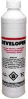
After exposure you have to remove the sensitized photoresist in order to unprotect the copper to remove. This process is called developing. Possible developer solutions include the following:
Laser printer toner carries with it a very high percentage of
pulverized plastic, which makes for an ideal etch resist. Ever
since laser printers became available, everyone has been searching
for a way of transferring a computer generated image directly to a
circuit card blank.
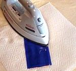
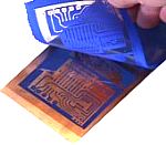
You first print your file to a special transfer paper
(Press-n-Peel) via a laser printer. Lay the image side face down
over a cleaned circuit board blank and then iron it for a minute or
two. The board then goes into a water bath that dissolves the
special coating allowing the paper to slide away leaving the toner
on the board… ready to etch!
The trace widths can be down to .006".
If a transfer error occurs, (it can happen on occasion), just wipe
the toner off the copper board with acetone, re-print the circuit
pattern and transfer again.
You could try this method using normal paper instead of special
paper but the results are not the same.
This method is easy, quick and inexpensive but is not adequate for
complex images.
Silkscreen
Definently not in the definition of “quick-prototyping”. This
process is only practical for mass production of a large number of
boards. You have the same basic requirements as that of the
photographic process described above with the only difference
being, instead of applying an emulsion to each and every circuit
board, you only expose and develop a screen which has been coated
with a photo-sensitive material. It’s fun to play with if you’ve
never done it before and a real eye-opener into the myriad of
applications that silk screening can be used for. This is the same
process to make a T-Shirt.
After exposing the screen, you place the PCB under the frame, load
in your special ink into the top of the frame and rake across the
frame. Where the screen is “open”, ink falls through to the board.
Lift the frame and let the board dry (…a long time!) before you can
etch it. They’re neat to play with if you’ve never done this
before. The silkscreen method ensure fastest and medium quality
reproduction.
There are several hobby kits on the market available at your local
art supply store. Consider this process only for a limited mass
production job. It’s just too much work for making just one
board.
Direct
Plating
It’s an industrial process to direct plating the board were do you
need a track. This method need very expensive industrial
machine.
It’s a very easy way to create prototypes. With a very expensive
cutter plotter for PCBs and a PCB layout software you could direct
“print” your circuit. The PCB printing is very slow, hence, is
indicated only to produce prototypes.
Send
Out
This method consist to prepare the data that will actually be used
by the manufacturers and send to a Board House to make a
professional PCBs.
The data for the manufacturer normally include layout file,
fabrication and assembly drawings, NC drill file of hole positions.
All data files must be in adequate format so, contact your board
house to know their requirements. Board Houses are ABSOLUTELY
necessary in the process of developing a board intended for mass
production, their board will be identical to the commercially made
prototype. This method is very expensive (you have to order minimum
quantity) and slow (wait a week or two). The result is an high
quality professional PCB complete with all the amenities (fine line
traces, solder mask, plated-thru holes and a parts insertion layer
screen printed on top).
If you want to produce only few prototypes PCBs this is not the
right method.
Final work
[Cleaning]
Cleaning
 In order to proceed
with others process you must clean your PCB.
In order to proceed
with others process you must clean your PCB.
Dirt obstacles your work, hence, it is an absolute necessity to
ensure that PCB are free from grease, oxidation and other
contamination.
Do not clean your board until you are ready to drill or to make
other process because resist protects the board from oxidation.
Use acetone or alcohol to remove resist. Clean copper board with
steel wool, S.O.S. or Brillo pads under running water. Rinse
cleaned board with soap and water. Be sure to remove all soap
residue. Dry thoroughly with lint-free cloth. Be sure to scrape any
burrs that appear on the edge of the board that may have resulted
from the cutting/shearing process.
PCB will generally oxidise after a few months, especially if it has
been fingerprinted, and the copper strips can be cleaned using an
abrasive rubber block, like an aggressive eraser, to reveal fresh
shiny copper underneath.
Also available is a fibre-glass filament brush, which is used
propelling-pencil-like to remove any surface contamination. These
tend to produce tiny particles which are highly irritating to skin,
so avoid accidental contact with any debris. Afterwards, a wipe
with a rag soaked in cleaning solvent will remove most grease marks
and fingerprints.
After preparing the surfaces, avoid touching the parts afterwards
if at all possible.
Tin
Plating
Tin-plating a PCB makes it a lot easier to solder, and is pretty
much essential for surface mount boards. Unless you have access to
a roller-tinning machine, chemical tinning is the only option.
Unfortunately, tin-plating chemicals are expensive, but the results
are usually worth it.
If you don’t tin-plate the board, either leave the photoresist
coating on (most resists are intended to act as soldering fluxes),
or spray the board with rework flux to prevent the copper
oxidising.
I suggest to use room-temperature tin plating crystals, which
produce a good finish in a few minutes. There are other tinning
chemicals available, some of which require mixing with acid, or
high-temperature use.
Made-up tinning solution deteriorates over time, especially in
contact with air, so unless you regularly make a lot of PCBs, make
up small quantities at a time (just enough to cover a PCB in the
tinning tray) keep the solution in a sealed bottle (ideally one of
those concertina-type bottles used for some photographic solutions
to exclude air), and return it to the bottle immediately after use
- a few days in an open tray and it can deteriorate badly. Also
take care to avoid contamination, which can very easily render the
solution useless. Thoroughly rinse and dry the PCB before tinning,
keep a special tray and pair of tongs specifically for tinning, and
rinse them after use. Do not top-up used solution if it stops
tinning - discard it and make up a fresh solution.
Ensure the temperature of the tinning solution is at least 25°C,
but not more than 40°C - if required, either put the bottle in a
hot water bath, or put the tinning tray in a bigger tray filled
with hot water to warm it up. Putting a PCB in cold tinning
solution will usually prevent tinning, even if the temperature is
subsequently raised.
Preparation is important for a good tinned finish - strip the
photoresist thoroughly - although you can get special stripping
solutions and hand applicators, most resists can be dissolved off
more easily and cleanly using methanol (methylated spirit). Hold
the (rinsed and dried) PCB horizontal, and dribble few drops of
methanol on the surface, tilting the PCB to allow it to run over
the whole surface. Wait about 10 seconds, and wipe off with a paper
towel dipped in methanol. Rub the copper surface all over with wire
wool (which gives a much better finish than abrasive paper or those
rubber ’eraser blocks’) until it is bright and shiny all over, wipe
with a paper towel to remove the wire wool fragments, and
immediately immerse the board in the tinning solution. Take care
not to touch the copper surface after cleaning, as fingermarks will
impair plating.
The copper should turn a silver colour within about 30 seconds, and
you should leave the board for about 5 minutes, agitating
occasionally (do not use bubble agitation). For double-sided PCBs,
prop the PCB at an angle to ensure the solution can get to both
sides.
Rinse the board thoroughly, and rub dry with paper towel to remove
any tinning crystal deposits, which can spoil the finish. If the
board isn’t going to be soldered for a day or two, coat it with
flux, either with a rework flux spray or a flux pen.
Drilling
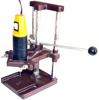
![]()
To make holes on your PCB you need a drill, a good vertical drill
stand and drill bits.
To drill fibreglass (FR4) board you must use tungsten carbide
drill bits because fibreglass eats normal high-speed steel
(HSS) bits very rapidly. Although HSS drills are good for odd
larger sizes (>2mm) that you only use occasionally where the
expense of a carbide isn’t justified. Carbide drill bits are
expensive, and the thin ones snap very easily. To avoid drill bits
break you must use a good vertical drill stand. Carbide drill bits
are available as straight-shank (i.e. the whole bit is the diameter
of the hole), or thick (sometimes called ’turbo’) shank, where a
standard size (typically about 3.5mm) shank tapers down to the hole
size. I much prefer the straight-shank type because they break less
easily, the longer thin section providing more flexibility.
When drilling with carbide bits, it’s important to hold the pcb
down firmly, as the drill bit can snatch the board upwards as it
breaks through, and this will usually break the bit if the board
isn’t held down.
Small drills for PCB usually come with either a set of collets of
various sizes or a 3-jaw chuck - sometimes the 3-jaw chuck is an
optional extra, and is worth getting for the time it saves changing
collets. For accuracy, however, 3-jaw chucks aren’t brilliant, and
small drill sizes below 1mm quickly form grooves in the jaws,
preventing good grip. Below 1mm you should use collets, and buy a
few extra of the smallest ones, keeping one collet per drill size,
as using a larger drill in a collet will open it out so it no
longer grips smaller drills well. Some cheap drills come with
plastic collets - throw them away and get metal ones.
You need a good strong light on the board when drilling to ensure
accuracy. It can be useful to raise the working surface about 15 cm
above normal desk height for more comfortable viewing. Dust
extraction is nice, but not essential - an occasional blow does the
trick! Note that fibreglass dust & drill swarf is very abrasive and
also irritating to the skin. A foot-pedal control to switch the
drill off and on is very convenient, especially when frequently
changing bits.
Typical hole sizes : ICs, resistors etc. 0.8mm. Larger diodes, pin
headers etc, : 1.0mm, terminal blocks, trimmers etc. 1.2 to 1.5mm.
Avoid hole sizes less than 0.8mm unless you really need them.
Always keep at least 2 spare 0.8mm drill bits, as they always break
just when you need a PCB really urgently. 1.0 and larger are more
resilient, but one spare is always a good idea.
When making two identical boards, it is possible to drill them both
together to save time. To do this, carefully drill an 0.8mm hole in
the pad nearest each corner of each of the two boards, getting the
centre as accurate as possible. For larger boards, drill a hole
near the centre of each side as well. Lay the boards on top of each
other, and insert an 0.8mm track pin in 2 opposite corners, using
the pins as pegs to line the PCBs up. Squeeze or hammer the pins
into the boards, and then insert and squeeze pins into the
remaining holes. The two PCBs will now have been ’nailed’ together
accurately, and can be drilled together. Standard track pins are
just the right length to fix the PCBs together without potruding
below the bottom board.
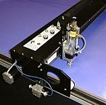
Automatic
An automatic drilling machine is very expensive tool so normally
it’s used only by manufacturer. The first step to automatic
drilling is generating the NC drill file of hole positions. This
file is usually in ascii format so that the drilling machine or
human can read it to produce your board. If you can’t produce a
drill file you can optically input the data but this method is more
expensive and error prone to use the manual method.
Cutting
In order to cut the PCB you must use different tools:
Ordinary saws (bandsaws, jigsaws, hacksaws): must be carbide
tipped to avoid blunted. The dust can cause skin irritation. It’s
also easy to accidentally scratch through the protective film when
sawing, causing photoresist scratches and broken tracks on the
finished board.
A carbide tile-saw blade in a jigsaw might be worth a
try.
Guillotine: is very useful, as it’s by far the easiest way
to cut fibreglass laminate. If you have access to a sheet-metal
guillotine, this is also excellent for cutting boards, providing
the blade is fairly sharp.
To make cut-outs, drill a series of small holes, punch out the
blank and file to size. Alternatively use a fretsaw, but be
prepared to replace blades often.
Through
Plating
When laying out double-sided boards, give some thought to how top
connections will be made. Some components (e.g. resistors,
unsocketed ICs) are much easier to top-solder than others (radial
capacitors), so where there is a choice, make the top connection to
the ’easier’ component. For socketed ICs, use turned-pin sockets,
preferably the type with a thick pin section under the socket body.
Lift the socket slightly off the board, and solder a couple of pins
on the solder side to tack it in place, and adjust so the socket is
straight. Solder all the solder side pins, then solder the required
top-side pins by reheating the joint on the solder side, while
applying solder to the pin and track on the component side, waiting
until the solder has flowed all round the pin before removing the
heat
![]() For vias
(holes which link sides without components), use 0.8mm snap-off
linking pins (shown left), available from most electronics
suppliers. These are much quicker than using pieces of wire. Just
insert the bottom of the stick into the hole, bend over to snap off
the bottom pin, repeat for other holes, then solder both sides.
For vias
(holes which link sides without components), use 0.8mm snap-off
linking pins (shown left), available from most electronics
suppliers. These are much quicker than using pieces of wire. Just
insert the bottom of the stick into the hole, bend over to snap off
the bottom pin, repeat for other holes, then solder both sides.
![]() If you
need ‘proper’ through-plated holes, for example to connect to
inaccessible top-side pins, or for underneath surface mount devices
(linking pins stick out too much for use here), Multicore’s
“Copperset” system (available from Farnell) works well, but the kit
is very expensive. It uses ‘bail bars’ (pictured left), which
consist of a rod of solder, with a copper sleeve plated on the
outside. The sleeve is scored at 1.6mm intervals, corresponding to
the PCB thickness. The bar is inserted into the hole using a
special applicator, and bent over to snap off the single bail in
the hole. It is then punched with a modified automatic
centre-punch, which causes the solder to splay over the ends of the
plated sleeve, and also pushes the sleeve against the side of the
hole. The pads are soldered each side to join the sleve to the
pads, and then the solder is removed with braid or a solder sucker
to leave a clear plated hole.
If you
need ‘proper’ through-plated holes, for example to connect to
inaccessible top-side pins, or for underneath surface mount devices
(linking pins stick out too much for use here), Multicore’s
“Copperset” system (available from Farnell) works well, but the kit
is very expensive. It uses ‘bail bars’ (pictured left), which
consist of a rod of solder, with a copper sleeve plated on the
outside. The sleeve is scored at 1.6mm intervals, corresponding to
the PCB thickness. The bar is inserted into the hole using a
special applicator, and bent over to snap off the single bail in
the hole. It is then punched with a modified automatic
centre-punch, which causes the solder to splay over the ends of the
plated sleeve, and also pushes the sleeve against the side of the
hole. The pads are soldered each side to join the sleve to the
pads, and then the solder is removed with braid or a solder sucker
to leave a clear plated hole.
![]() Fortunately, it is possible to use this system for plating standard
0.8mm holes without buying the full kit. You can buy the bail bars
seperately as refills. For the applicator, use a 0.9mm automatic
pencil, which actually works much better than the original
applicator, as you get one bail for every press of the button, and
it has a metal nose instead of the original plastic one. Get a
small automatic centre-punch, and grind the tip off so it’s
completely flat - this works fine for punching the bails. For an
anvil, use a thick flat piece of metal - the back of a large
heatsink is perfect for this - plate all the holes before fitting
any components so the bottom surface is completely flat. Holes must
be drilled with a sharp 0.85mm carbide drill to get the hole size
right for the plating process.
Fortunately, it is possible to use this system for plating standard
0.8mm holes without buying the full kit. You can buy the bail bars
seperately as refills. For the applicator, use a 0.9mm automatic
pencil, which actually works much better than the original
applicator, as you get one bail for every press of the button, and
it has a metal nose instead of the original plastic one. Get a
small automatic centre-punch, and grind the tip off so it’s
completely flat - this works fine for punching the bails. For an
anvil, use a thick flat piece of metal - the back of a large
heatsink is perfect for this - plate all the holes before fitting
any components so the bottom surface is completely flat. Holes must
be drilled with a sharp 0.85mm carbide drill to get the hole size
right for the plating process.
Note that if your PCB package draws pad holes the same size as the
drill size, the pad hole can come out slightly larger than the
drilled hole (e.g. from over-etching or non-centred drilling),
causing connection problems with the plating. Ideally, the pad
holes should be about 0.5mm (regardless of hole size) to make an
accurate centre mark. I usually set the hole sizes to exactly half
the drill size, so I know what the ‘real’ sizes should be when
sending NC drill data for production PCBs.
Draw Silkscreen
legend
Silkscreen legend is text and lines representing the parts on the
PCB. These are printed onto the board using the same process used
to print t-shirts. The color of the ink used is usually white,
although other colors are sometimes available on special order. The
part outlines will normally need to be trimmed to keep the lines
off pads and vias. Reference designators will need to be moved to
do the same and also to ensure they can be seen when the part is
installed. There may also be company logos, part numbers, or other
custom text or lines that need to be placed on the legend. Some
ECAD programs will automatically do the trimming.
With the same silkscreen method you can make a solder mask.
Solder mask is a special coating on top of the copper to keep out
moisture and protect the traces. Solder mask must have clearance
areas around the pads to keep the material from touching the pad,
making it difficult to solder. The material is usually green in
color, although other colors may be available on special order.
Soldering
Soldering is the process of fastening a part lead to a PCB. It uses
heat to melt a metallic compound around the lead and onto the
copper pad of the board.
Click here
to view the Basic Soldering Guide written by Alan
Winstanley.
- Engineering Express (www.expresspcb.com): Tips For Making PC Boards
- Mike’s Electric Stuff (www.electricstuff.co.uk): How to make really good homebrew PCBs
- CREATING A CIRCUIT BOARD FOR A THEREMIN OR IN GENERAL (www.ccsi.com/~bobs/mkboard.php)
- Nordic Shorwave Center (www.nordicdx.com): Steam your PC Boards
- Think & Tinker, Ltd. (www.thinktink.com): Mechanical Etching Bits
- Techniks Inc. (www.techniks.com): Press-n-Peel Transfer Film
- WebElectric Magazine (members.nccw.net/webe):Practical Surface Mount ; Inexpensive Printed Circuit Boards
- AirBorn Electronics (airborn.com.au): Printed Circuit Board (PCB) Etching ; The Printed Circuit Board (PCB) Layout
- Kepro circuits systems Inc. (www.turnpike.net/~Kepro): Instructions for Kepro’s SODIUM Persulphate ETCHANTS
- Leonardo, Gateway to EE91 (leonardo.caltech.edu): Making a professional board…
- Designer’s Den (www.aracnet.com/~gpatrick)
- Instant PCB Fabrication (www.dynaart.com)
- Vermont Safety Information Resources Inc. (hazard.com): ALDRICH CHEMICAL – AMMONIUM Persulphate
- ANALOG DEVICES (www.analog.com): Ask The Applications Engineer-10